
The end of our tests, and the power supply is (mostly) performing at an excellent level! Our main concerns were voltage output regulation which it passed with no problems. I’m confident the supply is safe enough to power the motherboard and all of the peripherals. There are a few tests where we uncovered some issues, so let’s look at those in depth.
- Capacitive load (+5V and +12V)
- +5V voltage hold-up time
- +5Vsb current delivery
- +5Vsb hold-up time during power down
- +5Vsb short circuit test
Failures
Capacitive load
Both the +5V and +12V outputs were out of regulation during the capacitive load test. The +5V output had a 10,000 µF capacitor as a load, and the +12V output had a 1,000 µF capacitor. This test is really about seeing if the power supply can turn on with essentially short circuits at the outputs. Capacitors act as short circuits initially until charge is acquired, and their DC resistance increases until it is essentially an open circuit.
This is calculated as an RC time constant.

So the regulation issue could really just be that when the capacitors are fully charged, there is basically zero load on the power supply (other than the load I needed for the supply to start). This very light load might explain the poor regulation. I am a little confused as to why the supply wouldn’t start with just the capacitors as the load, though. It may be that the rate of current increase triggers overcurrent protection. There may be a couple of tests we can do to narrow down the cause.
+5V hold-up time
With a purely resistive load, the hold-up time looked OK. With the optical drive as a load, there was a significant drop in voltage, followed by a recovery, then followed by the falling slope.
We need to experiment some to see where this is coming from. I tried the test again with an IDE HDD as the only load, and I got a similar hold-up time as the power resistor load. It may be something peculiar with the optical drive as the only load on the supply, so I’ll disregard this for now. I’ll take another look at this once the system is fully assembled again.
+5V turn-off slope
Unlike the other voltage rails, the turn-off slope on the +5V output had two distinct portions. It dropped from the nominal +5V output to +4.4V in around 75ms, and then dropped to 0V in around 200ms. We’ll have to see how the outputs differ in the actual circuit to see why this behavior might be different.
+5Vsb current delivery
The ATX specification calls for a minimum of 720mA current capacity for the +5V standby output. If you recall, this voltage source is used for powering portions of the motherboard to allow it to respond to the soft power switch, wake-on events, and so on.
We were only able to get 250mA of current with a short-circuit. We’ll look at the circuit to see what’s going on. My guess is that it is deliberately being limited to 250mA. Dell knows what standby current is needed, so this could be where this supply differs from the ATX specification on purpose.
We know from the earlier research into how this model changed that at some point Dell included USB ports. The USB 1.0 standard allowed a maximum current draw of 500mA per port, but I’m not sure if older systems provided the +5V standby power to USB while the system was “off.” What I’m getting at is– maybe there was no need for anything over 250mA standby current in the Pro200n. I would be interested to see what power supply was used for the later model with USB, as a different supply with higher standby current might confirm this theory.
+5Vsb hold-up time
We saw an anomaly where the +5V standby output spiked to +5.8V when the AC power was removed. This shouldn’t happen, and that is outside of its regulation threshold which is a no-no. We’ll take a look at the circuit to see if something is at fault, or perhaps it is just a poorly implemented design.
Circuit design and components
We’ll briefly take a quick look at the overall layout of the PS-5201-1D and then look in detail at a few sections.
Components and layout
Let’s take a look at the PS-5201-1D and label some of the component locations:
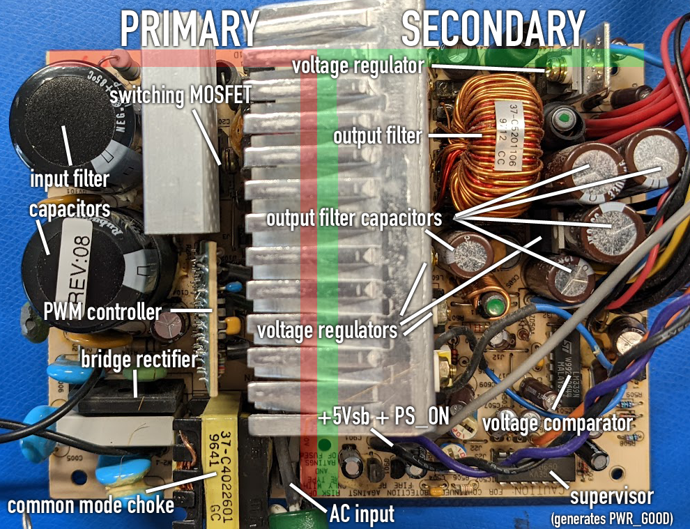
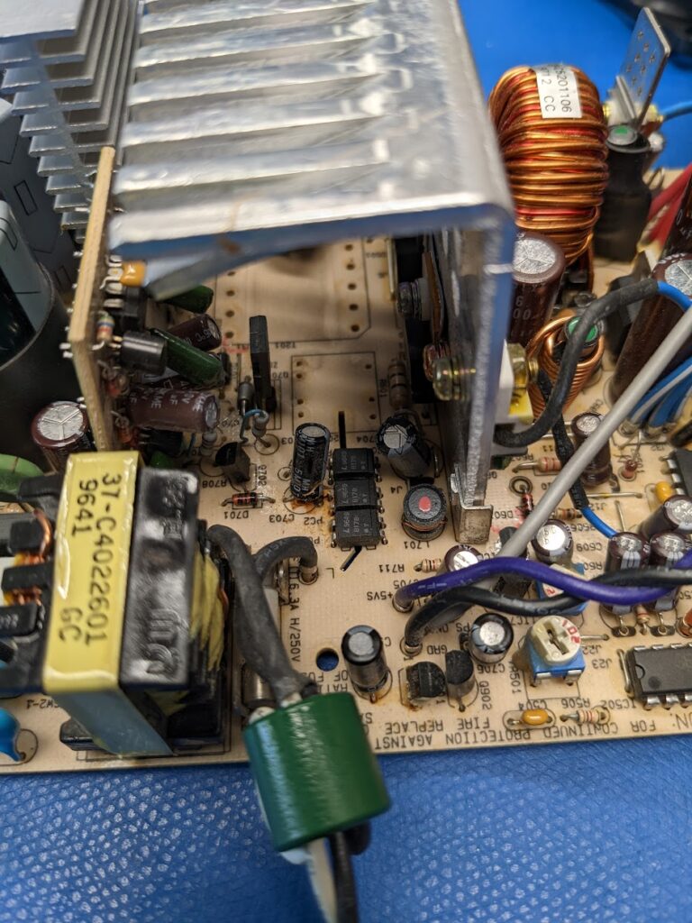
This power supply uses one switching element on the primary side making this a flyback converter topology.
The +5V standby supply uses a tiny transformer which we’ll look into later.
We’re mainly interested in the secondary side of the supply, so let’s focus there.
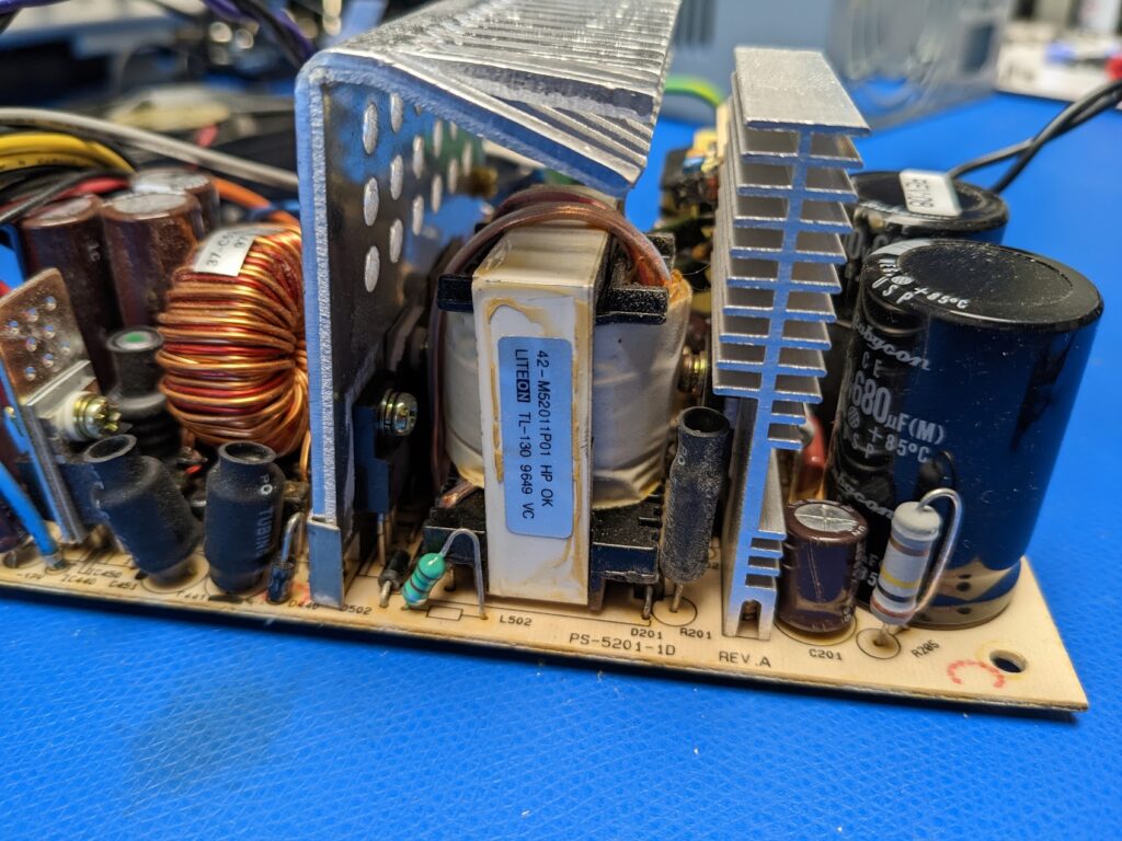
Transformers and rectifiers
Since we had a little bit of an odd result with the +5V output, we can take a look at how that particular output is generated and regulated. In order to do that, though, we’ll need to do some surgery.
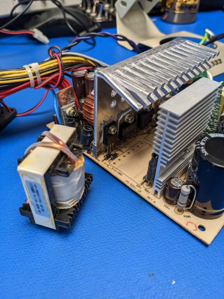
The output rectifiers mounted on the heatsink shown above couldn’t be seen in the overhead photo that is labeled.
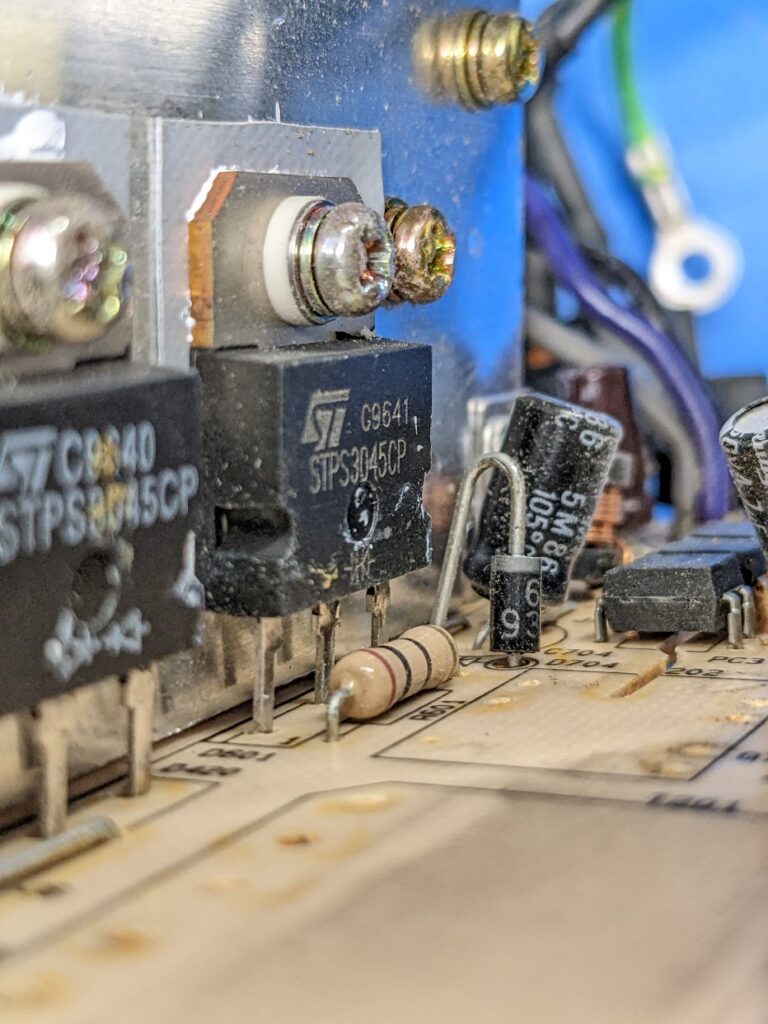
There are two ST STPS3045CP rectifiers: one for +5V and the other for +3.3V. These can each handle 15A per diode, or 30A per device. Remember the requirement of the +5V and +3.3V outputs not exceeding 140W total power draw? One of the reasons might be a temperature limitation since they’re both on the same heatsink.
+12V, -12V, and -5V
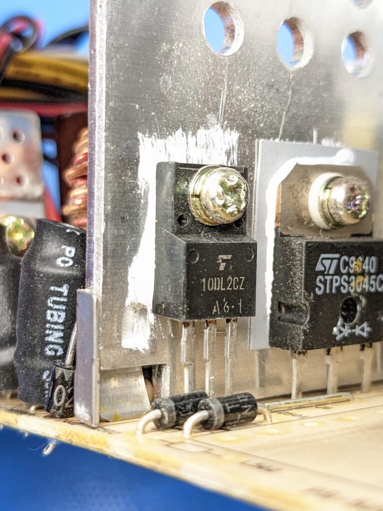
Also mounted on the heatsink, pictured above, is a Toshiba 10DL2CZ rectifier for the +12V output. This device can handle an average forward current of 10A, so plenty for our specified 6A limit.
The -12V and -5V are regulated using a pair of SEC KA7912 and KA7905 regulators respectively.
+5V
From the rectifier, the +5V output goes through the large output filter and a capacitor, and after that, another inductor and capacitor.
The two output capacitors are United Chemi-Con LXF series 3300µF 16V. They both tested with zero ESR and ~3200µF, perfectly healthy. This output is also connected to a LM339N comparator along with a 10µF capacitor which is also in great shape.
So how is the +5V output regulated? It is connected to an onsemi KA3501 supervisor IC (along with the +12V which it also monitors). One of the optoisolators mentioned earlier has its anode connected directly to the +5V output, and the cathode is connected to the feedback pin of the KA3501. The other side of the opto is connected to the primary-side PWM controller: an onsemi KA3843A. If the voltage drifts from +5V (if the load increases for instance), this will change the output of the optoisolator providing feedback to the PWM controller. It will then adjust the switching frequency to account for the change.
As for why the turn-off behavior is different compared to the 3.3V? It likely has something to do with how the +5V is used as feedback for regulation. I don’t think I’ll investigate any further though as the turn-off/hold-up behavior won’t have any impact to the performance of the supply.
+5Vsb
I also desoldered the standby transformer used for the +5V standby voltage.
The small rectangular outline is where the standby transformer was. You can also see the three optoisolators across the slot separating the primary and secondary sides of the supply. I think the TO-220 device just to the left of the transformer outline is a switching MOSFET for the standby.
It’s not easy to see, but there is a single diode next to the electrolytic cap inside the heatsink area, so I think this may also be a simple flyback converter topology. This diode is in series with a 31µH inductor, and there are two electrolytic capacitors in parallel, one on either side of the inductor. The +5V standby voltage is tapped off of the latter side of the inductor. There is no current limiting that I can determine on the secondary side of the standby circuit, so it is being done by the PWM controller.
The voltage spike we’re seeing on shut off is most likely due to the controller losing its reference. We might be able to counteract this by increasing the capacitance after the 31µH inductor. The capacitor there is 47µF, but increasing this to say, 100µF, might do the trick.
Next steps
Now that we’ve gotten a decent handle on how the power supply is designed and how it works, we can formulate a plan of action.
Despite the caps measuring OK, at least the ones I’ve desoldered so far, I think it’s a no-brainer to go ahead and replace them while the supply is disassembled. They won’t last forever, and it’s an easy and cheap way to ensure we won’t have any nasty failures in the coming years.
I’d like to run the board through an ultrasonic cleaner to get it looking brand new. There’s a bunch of old, dried up staking compound all over the board that needs to be removed as well.
The next update will include both of the above items and a quick look at the cooling fan as well.