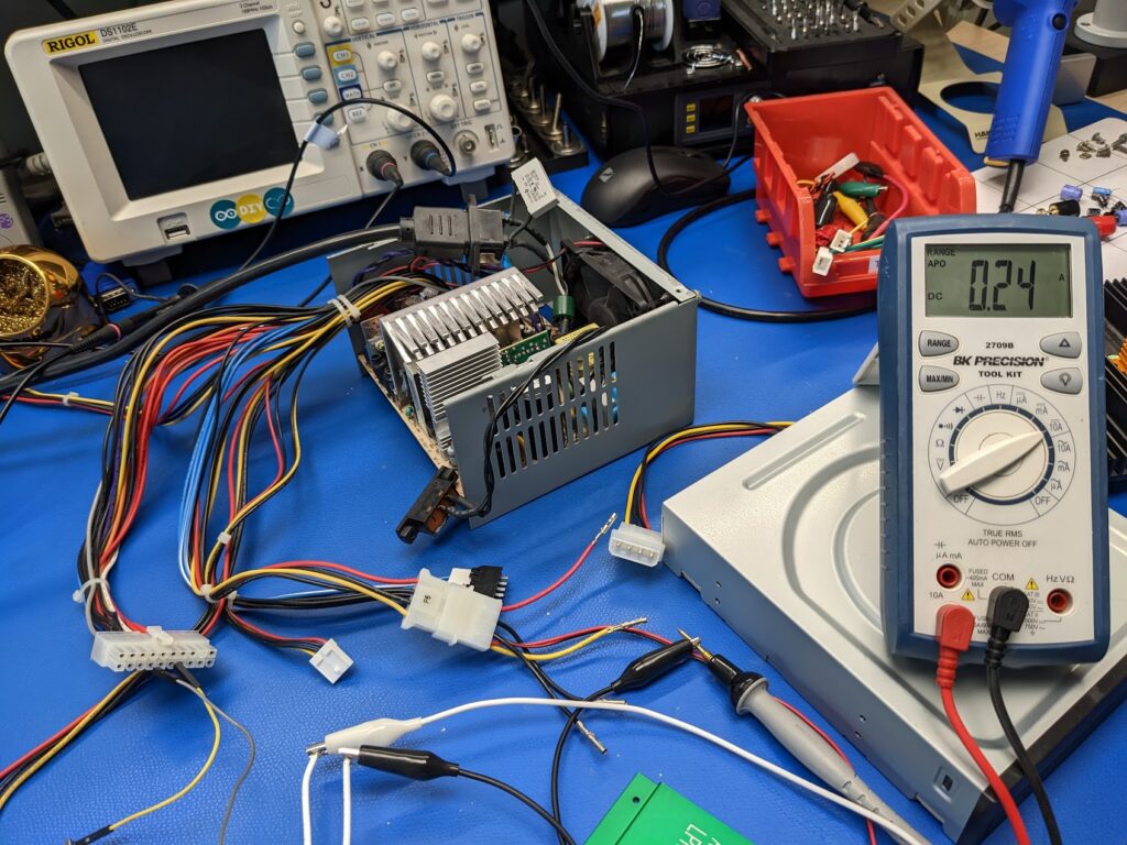
During testing, I’ll be powering the supply through an isolation transformer for safety, and will also use a variac to test the power supply with lower and higher AC voltages. For measurement, I’ll be using a Rigol DS1102E oscilloscope as well as a BK Precision 2709B digital multimeter. This is an entry-level scope with limited capabilities, but hopefully we’ll still be able to see some interesting results and learn a little.
Computer power supplies are switch mode power supplies and that means they have an inherent danger to them when testing. I always take extra precaution when working on them as mistakes can destroy your equipment, or even severely injure or kill you.
ATX power supply design guide
Even though this is not technically an ATX power supply due to the motherboard connector differences described above, we can safely assume that Lite-On designed it to ATX specifications since we know this model was used as a basis for ATX-compatible designs.
The earliest ATX power supply specification I’ve been able to find is from 1998 and is labeled as version 0.9. These were developed by Intel as guides for manufacturers to use when designing ATX-compatible power supplies. These guides are distinct from the actual specification versions. The ATX specification itself dates back to July 1995, with version 2.01 being released in February 1997. This power supply guide is based on version 2.02. Therefore, we know version 2.02 came out between 02/97 and 09/98. That means this guide is slightly newer than the Pro200n, but it’s not clear if that has any impact on specifications that are relevant to this power supply.
Regardless of that uncertainty, we’ll use this as a basis for testing as it’s the closest we’ve got. I’d be curious to see what power supplies other Dell models from this era used, or maybe slightly earlier than the Pro200n.
Testing
I thought it’d be neat to go through and test the power supply to see if it still meets the ATX specification. I won’t be able to test everything, but the goal is to ensure the supply will safely power the Pro200n for the next decade or more.
What tests can we run?
We want to test the supply to make sure it operates (mostly) in accordance with the ATX specification, but I have also have limitations around what I can safely test here in my lab. Here’s a rundown of what I think can be tested from the ATX spec:
- AC input voltage
- Input undervoltage
- DC voltage regulation
- Output ripple/noise
- Capacitive load
- +5V/+3.3V power sequencing
- Voltage hold-up time
- PWR_OK timing
- Power-on timing
- +5Vsb at AC power down
- Overshoot at turn-on/turn-off
- Short circuit protection
All of these tests will tell us a great deal about the condition of the supply, and should any of these tests fall out of spec, the specific test that failed will give us a clue of where to look for a problem.
I won’t be testing the absolute maximum rated outputs on the supply for a few reasons. I don’t want to stress something that is vintage and original to this system. We can load it with enough resistors and/or hardware to more or less simulate what a realistic load would be. This is where an electronic load would come in handy, especially one designed for multiple voltage rails, but those are definitely outside of the budget.
A small caveat is that I will be running the tests with the cover off because it’s simply going to be more convenient for me, but it shouldn’t make a large difference in the outcome.
With all that being said, let’s jump right into it! If interested, you may want to have the power supply design guide open so you can follow along with the requirements for each test.
AC input tests
AC input voltage
The power supply has a manual switch to designate either a 115VAC or 230VAC input. I don’t have a step-up transformer, so we’ll just be focusing on the 115VAC testing.
Section 3.1 states that the minimum acceptable input voltage is 90VAC, and it should be able to start up with this voltage under peak loading. The maximum voltage (115VAC nominal) is 135VAC. I don’t have the equipment to be able to alter the AC frequency, but those minimum and maximum values are specified as well.
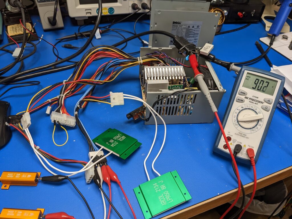
To test the minimum and maximum input voltage, I’ll be using a variac. This will allow me to alter the AC voltage going to the power supply. First, I’ll load the power supply with some power resistors, and maybe a fan or two on the +12V rail for an inductive load. All we’re looking for here is that the power supply starts under the minimum and maximum voltage.
I’ll be monitoring the input voltage using a multimeter at the power inlet on the supply.
90VAC input
Albeit not with peak load, but with a 1.65A load on the +3.3V and 1.25A on the +5V, the power supply started no problem at 90VAC input.
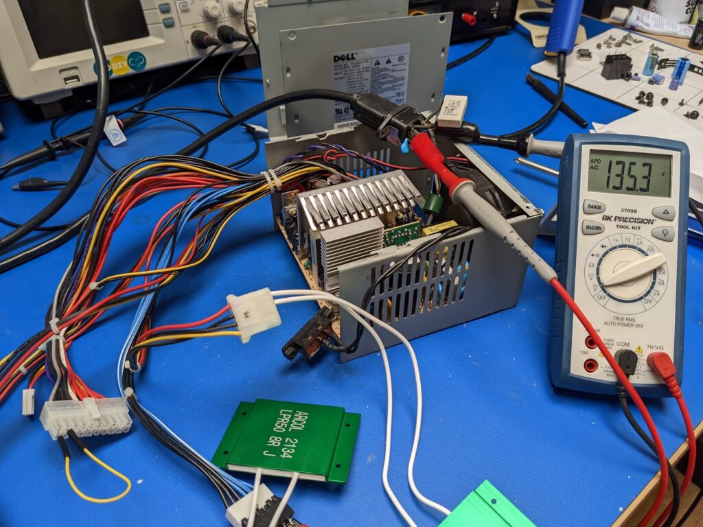
135VAC input
My variac has a slightly stepped-up winding to enable 140VAC output, so I could test the maximum required at 135VAC. It started up no problem:
Input undervoltage
I kept trying lower and lower AC voltage until I finally found that the supply wouldn’t start with anything under 56VAC. It did actually start with 56VAC though:
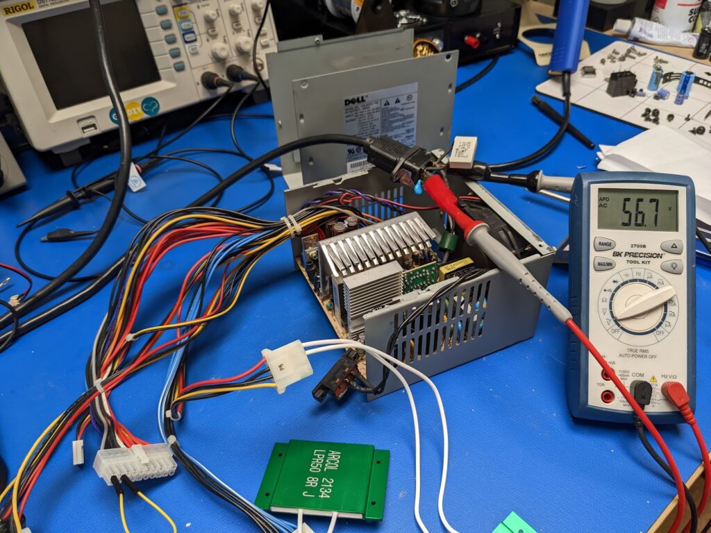
That being said, there was no obvious damage so I assume it passed this test, and by a large margin.
DC output tests
DC voltage regulation
The ATX specification provides a tolerance for each of the DC output voltages. Because of the nature of switch mode power supplies, the regulation should be worst at either near full load or without any load (or nearly any). The specification states the outputs should be within the tolerances specified under *all* line, load, and environmental conditions, so it doesn’t really matter either way as the supply should behave regardless.
Since I don’t have what’s needed to fully load the power supply, we’ll try using a small load on the +5V rail. I connected a 4 Ω resistor which will draw 1.25A, or 6.25W. I’ll use the oscilloscope to measure each voltage output, and will record the values below.
| OUTPUT | TOLERANCE | Vmin | Vmax | AVERAGE | MAX DEVIATION |
|---|---|---|---|---|---|
| +12VDC | ±5% | 11.8V | 12.2V | 12V | 1.7% |
| +5VDC | ±5% | 5.07V | 5.32V | 5.19V | 6.4% |
| +3.3VDC | ±5% | 3.36V | 3.46V | 3.41V | 5.2% |
| -5VDC | ±10% | -5.22V | -4.93V | -5.08V | 4.4% |
| -12VDC | ±10% | -12.5V | -12.2V | -12.35V | 4.2% |
| +5Vsb | ±5% | 4.97V | 5.01V | 4.99V | 0.6% |
My oscilloscope had bandwidth limiting on, with a 1X probe setting, DC-coupled, and I was using a small ground loop rather than the alligator clip lead. This reduces the loop area and hopefully reduces the amount of EMI being picked up. I was measuring at a 4-pin Molex or ATX connector for each reading about 8″ away from the power supply itself. The average voltage of each rail was well within the specification. The min and max did fall outside of the tolerance for several rails, however, this was due to noise which was easy to see on the scope. We’ll take a closer look at that in the next test.
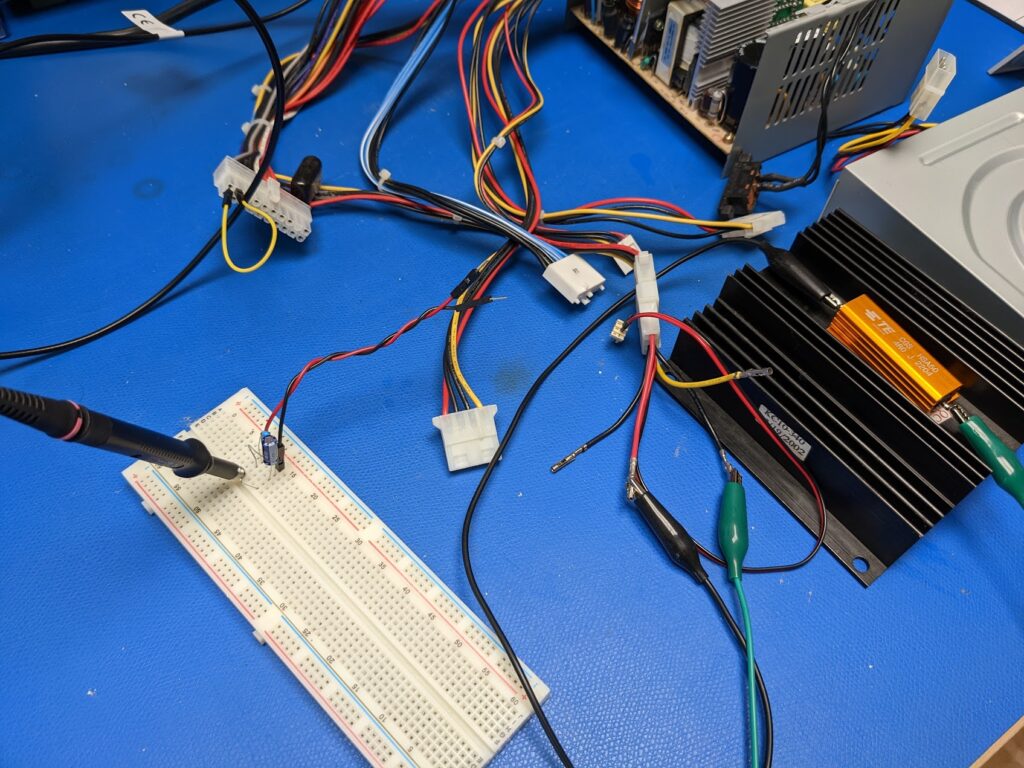
Output ripple / noise
For this test, the ATX specification has a few requirements:
- Ripple and noise are defined as periodic or random signals over a frequency of 10 Hz to 20 MHz.
- Measurements should be made with an oscilloscope with 20 MHz bandwidth.
- Outputs should be bypassed at the connector with a 0.1µF ceramic disk capacitor and a 10µF electrolytic capacitor to simulate system loading.
We’ll set the oscilloscope to AC-coupled as we only want to see the ripple and noise, since we already looked at the DC voltage regulation in the previous test. This means that the oscilloscope will block DC voltages and will only show us voltage changes, which is exactly what we want to see.
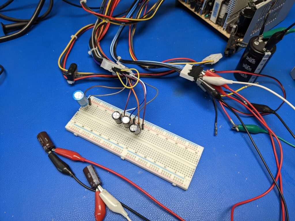
To make testing easier, I’m going to use a breadboard with the specified capacitors in parallel:
I’ll record the highest peak-to-peak voltage measured by the oscilloscope for each voltage rail:
| OUTPUT | MAX ALLOWABLE | ACTUAL |
|---|---|---|
| +12VDC | 120mVpp | 55.2mVpp |
| +5VDC | 50mVpp | 25.6mVpp |
| +3.3VDC | 50mVpp | 13.6mVpp |
| -5VDC | 100mVpp | 30.4mVpp |
| -12VDC | 120mVpp | 26.4mVpp |
| +5Vsb | 50mVpp | 41.6mVpp |
The bypass capacitors make a huge difference in the output. Compare the above values to the Vmin/Vmax values in the regulation tests. This makes sense, and this is realistic to the type of loads that this power supply would see.
Capacitive load
This is a test that measures how the supply will handle a purely capacitive load at startup. Capacitors act like short circuits when first energized, and this places a large current load on the output of the supply. Here’s what the ATX specification defines for the test:
| Output | +12VDC | +5VDC | +3.3VDC | -5VDC | -12VDC | +5Vsb |
|---|---|---|---|---|---|---|
| Capacitive load (µF) | 1000 | 10000 | 6000 | 350 | 350 | 350 |
Why the heck were some of these values chosen? They are odd ball, but we can make it work. Capacitance, unlike resistance, is additive in parallel. So in other words, if we connect two 3000µF capacitors in parallel, this is equivalent to 6000µF.
I don’t have any 330 or 350µF caps, but I do have many 470µF caps. We’ll use these in lieu of the 350µF as it will be a tougher test for the supply anyway.
The setup was as follows:
| Output | +12VDC | +5VDC | +3.3VDC | -5VDC | -12VDC | +5Vsb |
|---|---|---|---|---|---|---|
| Capacitive load (µF) | 1000 | 10000 | 7800 | 470 | 470 | 470 |
Definitely a harder test on some rails. Curiously, the supply still needed a “normal” load to start, so I connected an optical drive. It started successfully, but several voltages were nearly out of spec:
| VOLTAGE | MEASURED (with multimeter) |
|---|---|
| +12VDC | +11.5VDC |
| +5VDC | +5.26VDC |
| +3.3VDC | +3.40VDC |
| -5VDC | -5.01VDC |
| -12VDC | -12.26VDC |
| +5Vsb | +5.01VDC |
Both the +12V and +5V were struggling to regulate in this scenario. This may not be a surprising result, but we’ll see when we look more into this.
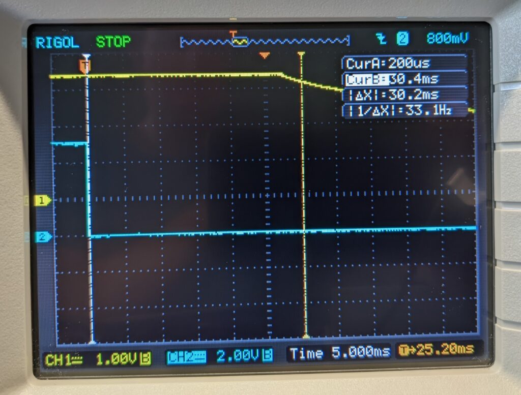
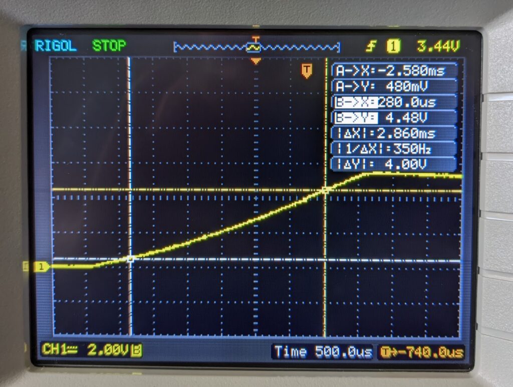
+5V/+3.3V power sequencing
This is an interesting requirement that specifies the +5V output must always be equal to or greater than the +3.3V output at all times whether during startup or normal operation. Additionally, the time between both of the rails reaching their minimum in-regulation level must be less than or equal to 20ms. In other words, let’s say the +3.3V rail reaches its nominal voltage first, in order to comply with this specification, the +5V rail must also reach its nominal voltage within 20ms of the +3.3V doing so, and vice versa.
For this we’ll employ the oscilloscope again, and we’ll use two channels.
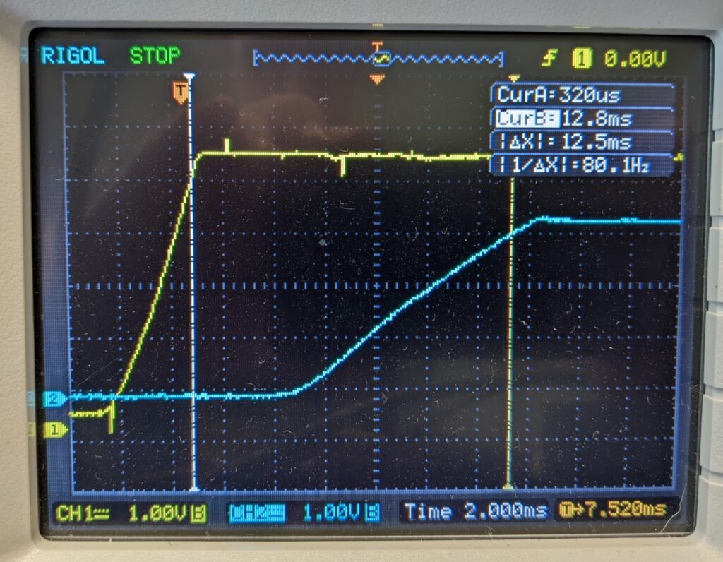
In the screenshot above, the cursors are positioned at the minimum acceptable regulated level for both voltage rails (4.75V and 3.14V respectively).
Our first requirement is that the +5V output is equal to or greater than the +3.3V at all times– and it is. The second requirement is that they both must reach their regulation within 20ms of each other– and they do (12.5ms).
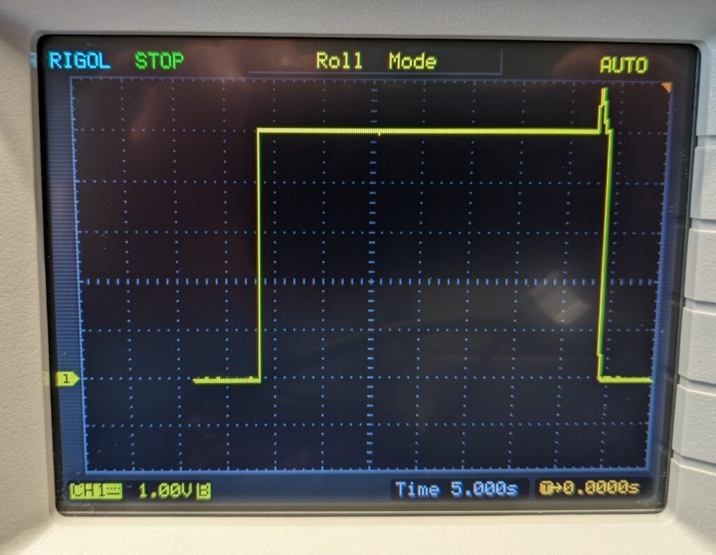
Voltage hold-up time
This is a requirement that essentially states the power supply has to continue to provide stable, regulated power for at least 17ms at full load. We can’t fully load the supply, so at first I used an optical drive and confirmed that the supply far exceeds 17ms:
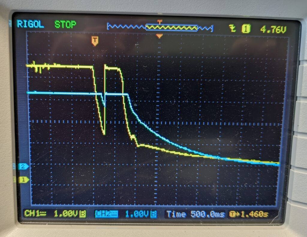
The +3.3V trace looks relatively normal except for the dip prior to the downward slope. I suppose the +5V behavior is due to discharging capacitors on the drive? I’m not entirely sure, so I swapped to a purely resistive load, and:
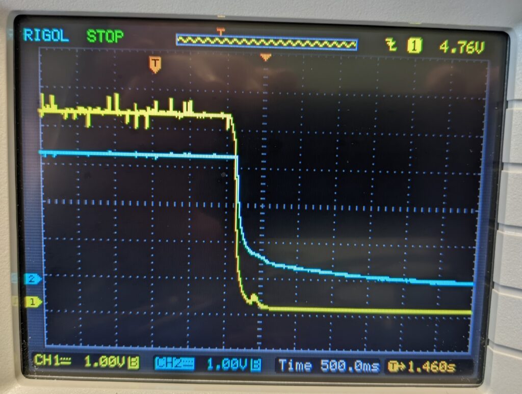
That looks mostly normal. The trigger point is at AC line cutoff, and the output persists for just over 1s. This behavior is probably different if the supply is fully loaded.
Timing / Housekeeping / Control tests
The timing of both the PWR_OK and PS_ON signals is defined in the ATX spec.
PWR_OK
The PWR_OK (also known as Power_Good) signal is a +5V TTL signal that is used as an output signifying that the power supply is outputting regulated +5V and +3.3V. In other words, this signal should not be present when either of those voltages are outside of their regulated thresholds or when the power supply is off. The actual voltage of PWR_OK can be between +2.4V and +5V– any value between those is considered a logic level high (as in “power output is good”).
PS_ON
The PS_ON signal conversely is an active-low signal. Its purpose is to allow the motherboard (or any external signal) to command the power supply to enable the DC voltage outputs. So in other words, PS_ON should be at a high level when AC power is present but the power supply is “off.” The ATX spec states that there should be an internal pull-up resistor which limits current on this pin, and there should be internal debounce circuitry to prevent repeated on/off activation from a mechanical switch (all switches will “bounce” between their states rapidly for a short period of time when actuated).
So in an ATX system, the power switch is bringing this PS_ON signal low (to ground)– it is a “soft” power button meaning you’re only switching this low voltage PS_ON signal and not the full +120VAC power as you would in an older AT power supply. I’ve been shocked by the latter and it is not a pleasant experience!
Timings
OK, so looking at the timing chart, we need to define a few timings:
- Power-on time — The time between when PS_ON is pulled low to when the +5V and +3.3V outputs are within their regulated thresholds. In the chart, this is between when PS_ON goes low and the end of T2 and it is defined as < 500ms.
- T2 — This is the risetime of the +5V and +3.3V outputs from <10% of nominal to the regulated threshold. This is defined as: 0.1ms ≤ T2 ≥ 20ms.
- T3 — This is a delay for the PWR_OK signal. Once the +5V and +3.3V outputs reach their regulated threshold, there should be 100ms ≤ T3 ≥ 500ms before PWR_OK begins to rise.
- T4 — When PWR_OK is brought low, there should be a delay before the +5V and +3.3V outputs drop out of their regulated thresholds. This is defined as T4 > 1ms.
- T5 — The PWR_OK signal should have a rise time T5 ≤ 10ms.
With those being defined, let’s get to testing!
Power-on time and T2
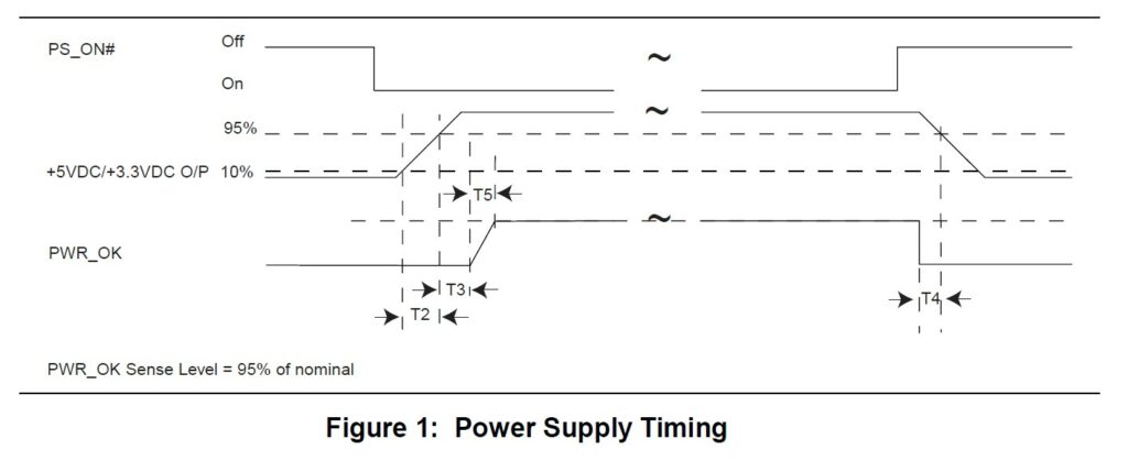
I only have a 2-channel scope, so we’ll just be able to monitor one voltage rail. Since we know the +3.3V is the last to rise and achieve regulation, we’ll use that one. We’ll be able to calculate both power-on time and T2 intervals in this test.
The above shows the +3.3V output in yellow (CH1) and the PS_ON signal in blue (CH2). We’re wanting to know the period of time between when PS_ON went low (which I triggered using a jumper wire to connect PS_ON to ground) and when the +3.3V output reached regulation (+3.14V). The cursors are at the respective positions, so we need to know the delta between them which is 113ms. It needed to be less than 500ms, so this test passes.
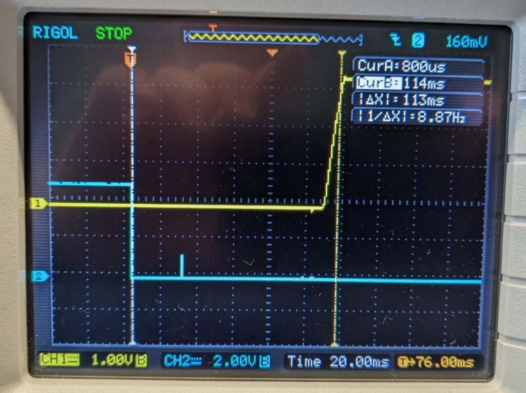
This is only showing the +3.3V output, and we see a rise time of 8.6ms, which is between the specified 0.1ms and 20ms. I checked the +5V output and it was around 3ms, so that was in spec as well.
T3
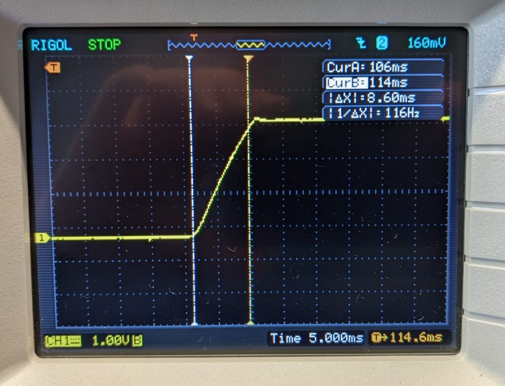
For this one, we’ll need to monitor the +3.3V output and the PWR_OK (also known as Power_Good) signal on the ATX connector. We’re looking for the delay between voltage regulation and PWR_OK rising.
We should have between 100ms and 500ms, and we’re at 236ms.
T4
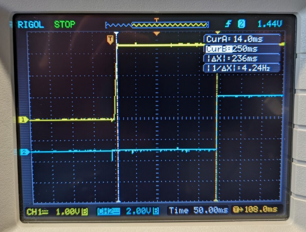
This is a similar test to the one above, except we’re on the other end: we want to see how long it takes for the +3.3V to drop out of its regulation threshold after PWR_OK is brought low.
So again, PS_ON is in blue and +3.3V is in yellow. We can see the +3.3V persists for 30ms after PS_ON goes low. This only needed to be above 1ms, so we’re set.
T5
No need to test this one, as we’ve seen in the last two tests that PWR_OK is pretty much instantaneous in its rise and fall time. It just needed to be less than or equal to 10ms, so no problems here either.
+5Vsb
Now we’ll take a quick look at the +5V standby output.
Current delivery
We first need to see what kind of current we can draw from this output. The specification states that it should be capable of delivering 720mA ± 5% (684mA to 756mA) at minimum, but they recommend having designs capable of delivering up to 1.5A.
For this test, we’ll use the multimeter in current mode, and we’ll first use a load of 8 Ω. This will draw 625mA (5V / 8 Ω). We won’t bother actually turning on the main voltage outputs as we’re just testing the standby supply here.
The power supply was only able to deliver 240mA. Not only that, but after shutting off the AC power, there was a very high frequency squeal that the supply was emitting as the capacitor, I’m assuming, on that rail discharged. Something doesn’t seem right, and it shouldn’t have any problems delivering higher power. We’ll have to take a look at the circuit itself to draw any more conclusions, though.
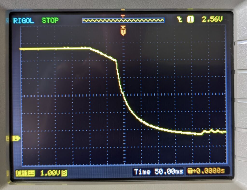
Hold-up time at AC power down
This is same test we did earlier (Voltage hold-up time), but for the standby supply. I’ll use the oscilloscope to measure this, and we’re looking for continuous +5V output for at least 17ms. The specification states it should be monotonic in nature where it drops to 0.0V without any perturbations.
The +5Vsb output lasted longer than 17ms alright… more like closer to 30s (forgot to mark the actual AC trigger point). There’s really nothing wrong with a long delay like this, but the spike before the drop is concerning. Let’s look in more detail:
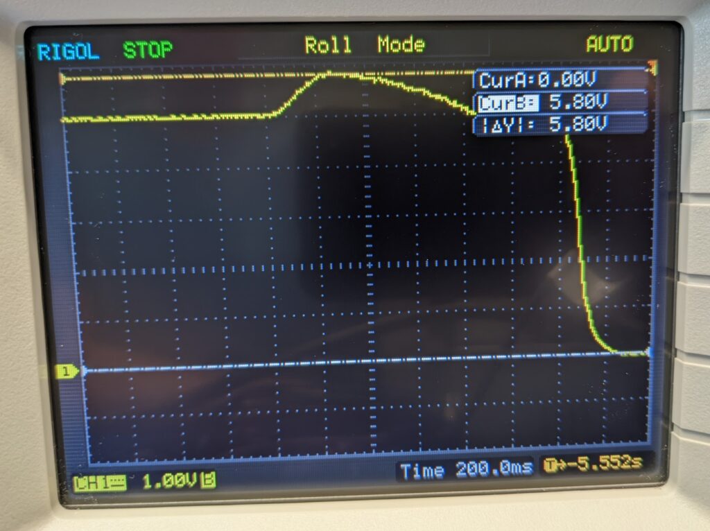
That’s not great. We see the output spiking to +5.8V before dropping in a non-linear fashion. The output spikes, drops back down to +5V, and then drops like we would expect.
This is an important finding because not all devices can withstand a spike that large. Some +5V devices will only accept up to +5.5V for example. On a standby circuit, this may not present a huge issue, but it’s definitely something that needs to be investigated further.
Overshoot at turn-on / turn-off
This sounds like a complicated test in the specification, but it’s really not. They’re simply looking for a smooth ramp-up and ramp-down of voltages during power-on and power-off respectively. The first requirement is that no voltages should overshoot their nominal voltage by 10% or more when AC power is applied or lost or when PS_ON is brought low or high.
Next, there should be a smooth and continuous ramp from 10% to 90% of the final voltage for each output. The slope of the turn-on waveform should have a value between 0 V/ms and [nominal V]/ 0.1ms.
Additionally, for any 5 ms segment of the 10%-90% ramp, a straight line drawn between the end points of the waveform in that segment must have a slope ≥ [nominal V]/20ms.
We’ve actually already seen the +3.3V rise and fall slopes, and they look like they’re correct. Looking back at the +5V, we may want to take another look. We’ll also test the +12V. I won’t bother with the negative voltages.
+5V
Here’s turn on:
And turn off:
Everything looks good with the turn on rise. The turn off isn’t perfect. Instead of a smooth, continuous fall, there is an initial fall with a distinct increase in rate at +4.4V. We have very small spikes at the tail end as well, but those are of no concern. This would ideally be a smooth, consistent line without a step like that.
+12V
The +12V rise and fall was pretty much perfect.
We may need to look further into the +5V fall behavior, especially because both the +3.3V and +12V rails do not exhibit this issue.
Short circuit protection
An easy test for our last– simply short each of the positive voltage rails to see how the supply reacts. The test is specified to use an output impedance of less than 0.1 Ω. The ammeter I’m using has an internal resistance of 0.08 Ω as measured by an LCR meter. I tried the measurement at different frequencies and got about the same result, so I think it’s OK to use.
| VOLTAGE | RESULT |
|---|---|
| +3.3VDC | PASS |
| +5VDC | PASS |
| +12VDC | PASS |
| +5Vsb | ??? |
An added requirement is that the +5Vsb output is supposed to be able to be shorted indefinitely. I encountered the same maximum current draw of 240mA as we did in the +5Vsb current delivery test. After cutting the power, the same high frequency squeal was emitted from the supply.
Conclusion
The next post will be the summary of our testing, as well as what failed and investigations into that. Stay tuned!